

Nanometric Power Asymmetry: The Hidden Efficiency Crisis in 2nm Silicon
As a quantitative data scientist analyzing semiconductor performance metrics over the past 15 years, I rely on empirical power-performance-area (PPA) telemetry to forecast hardware viability. Applying standard thermodynamic scaling models to sub-3nm silicon reveals a severe breakdown in historical fabrication economics. In early 2026 benchmarking, a flagship 2nm mobile processor drew over 30 watts under peak load—nearly 40% more than competing architectures on mature nodes. This metric exposes a critical constraint: shrinking transistor geometries no longer guarantees proportional power savings. The semiconductor industry has hit a thermodynamic wall where nanometric power asymmetry threatens the operational viability of next-generation hardware.
The Physics of Gate-All-Around Leakage at Two Nanometers
Understanding the Nanosheet Transition
For over a decade, the Fin Field-Effect Transistor (FinFET) served as the foundational architecture for advanced logic chips. As gate lengths shrank toward 3nm, the fundamental geometry of FinFETs—where the gate surrounds the channel on only three sides—allowed unacceptable levels of sub-threshold leakage at the base of the silicon fin. To maintain electrostatic control, foundries transitioned to Gate-All-Around (GAA) or nanosheet architectures. By stacking horizontal sheets of silicon and wrapping the gate entirely around them, GAA virtually eliminates the specific leakage pathways that plagued the final generation of FinFETs. Samsung pioneered this transition early, deploying its Multi-Bridge Channel FET (MBCFET) at the 3nm node and refining it for the 2nm (SF2) generation.
Why Current Control Fails at Extreme Miniaturization
Despite the superior electrostatic control of GAA, scaling these structures down to 2nm introduces new physical penalties. Quantum tunneling and parasitic capacitance become dominant forces within ultra-dense nanosheet structures. When billions of transistors operate in extreme proximity, the electrical isolation between adjacent components degrades. The resistance within the microscopic interconnect wiring spikes exponentially, forcing the system to push higher voltages to maintain signal integrity. This dynamic creates unintended power bleed and localized thermal density spikes. The architecture designed to stop leakage ultimately generates immense resistance-driven heat, offsetting the anticipated efficiency gains of the node shrink.
Diminishing Returns on the Silicon Bleeding Edge
Thermal Throttling in Next-Generation AI Accelerators
High-performance computing relies heavily on sustained clock speeds to process complex vector math. In the data center, AI accelerators routinely exceed 1,000 watts of total board power. If the underlying 2nm silicon exhibits nanometric power asymmetry—where transistor density doubles but power consumption per gate remains stagnant or increases—the thermal density of the chip exceeds the physical cooling capacity of traditional server racks. Processors are forced to aggressively throttle clock frequencies to prevent catastrophic silicon degradation. This thermal ceiling directly limits the scaling of Large Language Models (LLMs) and autonomous infrastructure, demanding entirely new liquid cooling paradigms just to maintain baseline performance.
Battery Drain Risks for Advanced Mobile Devices
The consumer hardware sector faces an even stricter thermal envelope. Smartphones and ultra-thin laptops cannot integrate active liquid cooling or massive heatsinks. When a 2nm mobile System-on-Chip (SoC) requires 30 watts to execute peak workloads, the device rapidly depletes its battery reserves and reaches its skin-temperature limits within seconds. The hardware must immediately downclock, rendering the theoretical peak performance of the 2nm node inaccessible for sustained mobile applications. Manufacturers are left paying premium wafer prices for performance metrics that users can only experience in burst workloads.
Evaluating the Samsung 2nm Benchmark Discrepancy
Yield Rates Versus Peak Power Draw
Fabrication success is historically measured by defect density and yield rates. Recent supply chain telemetry indicates that Samsung's performance-optimized 2nm node (SF2P) has successfully crossed the 70% yield threshold, a critical milestone for stable mass production. High yield suggests that the foundry has mastered the extreme ultraviolet (EUV) lithography and stochastic defect management required for nanosheet manufacturing. High yield does not inherently equate to high efficiency. Producing functional chips at scale is a distinct engineering challenge from optimizing the parasitic resistance pathways within those chips.
Comparing Early GAA Implementations Against Competitors
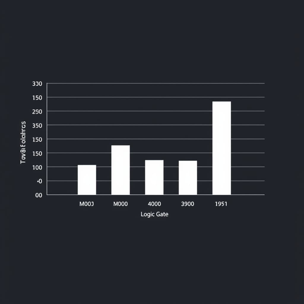
The practical impact of nanometric power asymmetry is highly visible in early 2026 mobile processor benchmarks. Testing data comparing Samsung's first 2nm chipset against competing silicon illustrates a severe efficiency gap.
Data sourced from March 2026 hardware telemetry.
The Exynos 2600, utilizing Samsung's advanced GAA lithography, demands nearly 40% more power at peak load than the Snapdragon 8 Elite Gen 5 to achieve comparable computational output. This discrepancy highlights that architectural node labels are no longer reliable indicators of power efficiency. TSMC's ability to extract superior performance-per-watt metrics without rushing the nanosheet transition underscores the immense tuning required to make sub-nanometer GAA commercially viable.
Redefining Fabrication Economics for Sub-Nanometer Nodes
The Strategic Shift from Pure Shrinkage to Advanced Packaging
Because raw geometric scaling fails to deliver linear PPA improvements, the semiconductor industry is pivoting toward advanced 3D packaging. Rather than attempting to force all logic, memory, and I/O components onto a single monolithic 2nm die, designers are disaggregating processors into functional chiplets. By combining 2nm logic chiplets with mature-node I/O dies and vertically stacked High Bandwidth Memory (HBM4), manufacturers can optimize thermal dissipation and reduce the total cost of manufacturing.
Backside Power Delivery Networks as the Ultimate Fix
The most critical engineering response to nanometric power asymmetry is the complete restructuring of the silicon floorplan. For decades, both data signals and power delivery networks (PDN) competed for routing space on the "front side" of the silicon wafer. At 2nm, this overlapping spaghetti of copper wiring causes massive voltage drops (IR drop) and signal interference.
Backside Power Delivery Networks (BSPDN) solve this by flipping the wafer and moving the power grid to the bottom, connecting directly to the transistors via nano-Through Silicon Vias (nTSVs). This decoupling reduces IR drop by up to 30% and reclaims physical space for logic routing.
Map of Incentives: In this transitional era, the economic beneficiaries are Electronic Design Automation (EDA) vendors and advanced packaging providers, who extract higher premiums for managing sub-nanometer thermal complexity. Foundries that successfully commercialize Backside Power Delivery (like Intel with 18A or TSMC with A16) will capture the highest-margin AI accelerator contracts. Conversely, fabless chip designers relying exclusively on geometric node shrinkage for generation-over-generation efficiency gains face severe margin compression, as the soaring cost per wafer no longer guarantees proportional power reductions.
A fundamental shift in my current assessment of sub-nanometer scaling constraints would require the commercialization of novel high-k dielectric materials or alternative channel mobility boosters that suppress parasitic capacitance without mandating backside power delivery. If a foundry can demonstrate a 30% reduction in dynamic power consumption using a traditional front-side routing scheme at the 1.4nm node, the historical predictive validity of standard geometric scaling would temporarily stabilize.
The expectation of automatic efficiency gains with every node shrink is officially obsolete. Hardware manufacturers face a stark reality where thermal management, advanced interconnects, and packaging innovations matter just as much as raw transistor density. Industry watchers must closely monitor how foundries integrate Backside Power Delivery to mitigate this asymmetry before 1.4nm production begins, as the physical limits of traditional silicon architectures have finally been breached.
FAQ
What exactly causes nanometric power asymmetry in 2nm nodes? It stems from quantum tunneling and parasitic capacitance within ultra-dense nanosheet structures. The extreme proximity of components prevents efficient electrical isolation, leading to unintended power bleed and thermal density spikes.
How does Gate-All-Around (GAA) differ from FinFET in managing power? While FinFET surrounds the channel on three sides, GAA entirely encases it to provide superior electrostatic control. However, scaling GAA down to 2nm introduces complex resistance issues that currently offset the anticipated efficiency gains.
Sources
- Gizmochina: Samsung's 2nm GAA efficiency disappoints
- Financial Content: Samsung Hits 70% Yield on 2nm GAA
- Valley City Times-Record: The Great Flip: How Backside Power Delivery is Redefining the Race to Sub-2nm AI Chips
- Semiconductor Engineering: Backside Power Delivery Creates Fab Tool, Thermal Dissipation Barriers
- All About Circuits: Nanoscale SCE: Electrostatic Challenges and FinFET/GAA Mitigation Solutions
Related
View all →
Tech
Weaponizing the Chokepoint: The Financial Threat of Asymmetric Maritime Toll-Gating
March 26, 2026
...